AI Supply Chain Revolution:TSMC Japan & The Hidden Power of Semiconductor Ecosystem

Image Caption:
A panoramic and aerial view of TSMC’s Kumamoto fab (JASM). The first plant is already in mass production (12–28nm, mainly for automotive and image sensors), while a second fab is under construction with plans to upgrade to an advanced 3nm process focused on AI chips. Total investment is expected to reach up to $17 billion. The site features multiple cleanroom buildings, surrounded by greenery and farmland, forming a new Taiwan–Japan semiconductor hub.
1. TSMC’s Core Strength: The Pure-Play Foundry Model
President Onodera emphasized that TSMC’s success is rooted in its pure-play foundry model. In the past, most chipmakers followed the IDM (Integrated Device Manufacturer) model, owning and operating their own fabs, often struggling with uneven capacity utilization.
TSMC founder Morris Chang introduced a groundbreaking idea:
focus exclusively on manufacturing chips for customers, without producing any in-house products.
This model delivers three key advantages:
- No competition with customers, building deep trust.
- No risk of IP leakage or internal capacity conflicts, since TSMC has no competing products.
- Flexibility across market cycles, allowing TSMC and its customers to navigate shortages and downturns together.
This approach enabled the rise of fabless companies such as NVIDIA and Apple, allowing them to focus entirely on design while outsourcing manufacturing to TSMC—accelerating innovation in AI, smartphones, automotive, and beyond.
A critical enabler is the Process Design Kit (PDK). Think of it as a highly detailed “manufacturing playbook” that includes design rules, models, and technical data. It allows customers to design chips optimized for advanced nodes—without accessing TSMC’s internal trade secrets. TSMC also provides a full design ecosystem to help optimize power efficiency, chip size, and performance.
2. TSMC’s Four Key Operations in Japan
- TSMC Japan (est. 1997): Customer support and coordination hub
- Japan Design Center (JDC): Advanced design support
- Kumamoto Fab (JASM): Mass production and ongoing expansion
- Tsukuba 3DIC R&D Center: Focused on advanced packaging (3D IC)

Image Caption:
A schematic of TSMC’s advanced packaging technologies (3D IC stacked architecture). Multiple layers of chips—such as logic dies and HBM (high-bandwidth memory)—are vertically integrated using CoWoS and SoIC technologies, enabling high-performance, low-power AI accelerators. This shift from 2D planar layouts to 3D stacking represents a transformative leap and a key enabler in the AI era.
3. Japan’s Semiconductor Material Suppliers: Hidden Champions of the Global Upstream
Japan dominates the global market for critical semiconductor materials such as silicon wafers and photoresists, with market shares ranging from 50% to 90%. These high-purity materials form the foundation of advanced semiconductor manufacturing, supporting not only TSMC’s Kumamoto fab but also cutting-edge production worldwide.

Image Caption:
A semiconductor-grade silicon wafer produced by Shin-Etsu Chemical. The image shows a massive 300mm single-crystal silicon ingot alongside mirror-polished wafers with ultra-smooth surfaces, demonstrating ppt-level purity control—the fundamental building block of all advanced chip manufacturing.
Japan holds a dominant position in semiconductor materials. Of the 19 key materials, around 14 have global market shares exceeding 50%, with some reaching as high as 70–90%. These materials underpin all chip production and are especially critical for advanced nodes (such as EUV and sub-2nm processes) as well as advanced packaging.
Major players include:
- Shin-Etsu Chemical: The world’s largest supplier of semiconductor-grade silicon wafers. Together with SUMCO, it commands over 50% of global market share. It also supplies photoresist materials and ultra-high-purity chemicals.
- SUMCO: The second-largest silicon wafer manufacturer globally, specializing in high-end 300mm wafers.
- JSR Corporation: A leading photoresist supplier, particularly strong in ArF and EUV resists.
- Tokyo Ohka Kogyo (TOK): A major photoresist manufacturer with a strong position in EUV resists. Japanese firms collectively account for roughly 87–91% of the global photoresist market.
- Others: Fujifilm, ADEKA, Toyo Gosei (photoresist materials), Namics (advanced packaging underfill), among others.
These companies are known for their extreme purity control (down to ppt levels) and a co-development model with customers, forming a tightly integrated supply chain with TSMC’s Kumamoto fab.
The key to their success lies in “growing together with customers”—deep involvement in process development that creates strong technological moats and customer stickiness. Even amid geopolitical risks (such as export controls), their long-term validation and unmatched purity make them difficult to replace.
4. Japan’s Semiconductor Equipment Suppliers: Enablers of Precision Manufacturing
Japanese equipment manufacturers dominate critical segments such as coating/developing, dicing, testing, and EUV inspection, with market shares often reaching 70–90%. These tools are indispensable to advanced wafer fabs.
Key companies include:
- Tokyo Electron (TEL): Holds 80–90% global share in coating and developing equipment, and also provides thermal processing, etching, CVD, and cleaning tools. One of the world’s top five semiconductor equipment companies, with close ties to TSMC and an R&D center in Kumamoto.
- Advantest: A leader in semiconductor test equipment (ATE), especially for AI and high-end memory.
- SCREEN Holdings: A benchmark in wet cleaning equipment, with nearly 50% global market share.
- Disco: Dominates wafer dicing and grinding equipment (70–80% share), essential for advanced packaging.
- Lasertec: Near-monopoly in EUV mask inspection systems.
Other important players:
- Kokusai Electric: Thermal processing and thin-film deposition equipment
- Hitachi High-Tech: Inspection and etching systems
- Tokyo Seimitsu (Accretech): Probe stations and dicing tools
- Canon / Nikon: Lithography equipment (serving niche markets outside EUV)
- Hidden champions: Rorze (wafer handling systems), Ebara (CMP equipment, global No. 2), among others
Japan’s Equipment Advantage and Global Impact
- Dominance in key segments: Coating/developing (TEL ~90%), dicing/grinding (Disco 70–80%), EUV inspection (Lasertec), and cleaning (SCREEN) are all essential steps surrounding lithography.
- Integration with TSMC Kumamoto: TSMC’s first fab in Kumamoto is already in mass production (12–28nm for automotive and image sensors), with a second fab planned for more advanced nodes (e.g., 3nm). Japanese equipment suppliers—especially TEL—play a major role, with local R&D presence strengthening Taiwan–Japan collaboration. Strategic investors like Sony, Denso, and Toyota further reinforce the ecosystem.
- Driven by AI and advanced packaging: Demand for HBM and CoWoS has significantly increased the need for dicing, testing, and cleaning equipment. Japanese suppliers are expanding capacity and accelerating R&D, with strong order visibility extending into 2027.
- Supply chain resilience: The combination of Japanese materials and equipment forms a highly defensible ecosystem that is difficult to replicate. Even under geopolitical pressure, their precision engineering and co-development approach sustain competitiveness.
The success of Japan’s equipment makers mirrors that of its materials suppliers: deep collaboration with customers. By embedding themselves into process development, their tools become an integral part of technological evolution—complementing material leaders like Shin-Etsu, JSR, and TOK, and collectively supporting the global semiconductor industry.
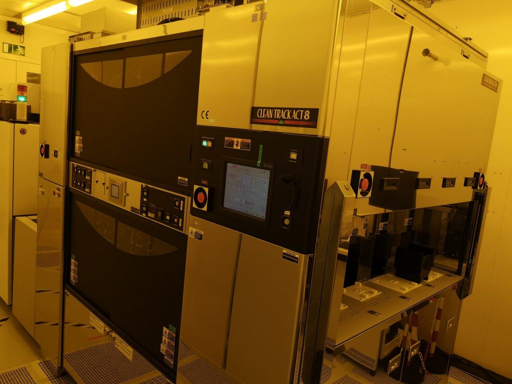
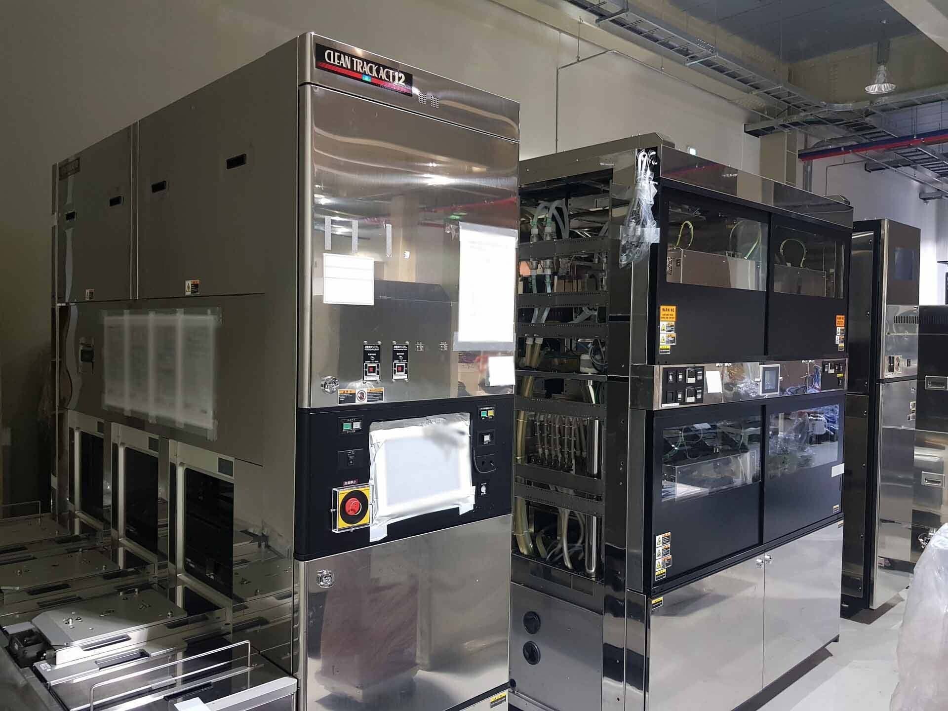
Image Caption:
Tokyo Electron (TEL) CLEAN TRACK ACT series spin coater and developer system. Inside a cleanroom environment, silicon wafers are rapidly rotated to achieve uniform photoresist coating and development, a critical preparatory step before EUV lithography.


留言
張貼留言