Quantum Boundary Warfare: How TSMC’s A14 (1.4nm) Breaks the 1nm Wall and Unlocks the AI Holy Grail
TSMC’s A14 (1.4 nm) process is widely regarded as one of the “final frontiers” of semiconductor physics—and a critical technological “holy grail” underpinning the global AI era. As fabrication scales push into the angstrom regime, engineers are no longer merely optimizing materials; they are confronting the laws of quantum mechanics head-on. Scheduled for mass production around 2028, this technology aims to meet the explosive demand for AI compute while delivering substantial gains in performance and energy efficiency.
Below is a comprehensive, illustrated article integrating the latest official disclosures, technical analyses, and detailed mathematical models of quantum tunneling (based on public information such as TSMC’s 2025 North America Technology Symposium, as of early 2026):
1. The Physical Limit: Quantum Tunneling — The Challenge of the 1 nm Wall
At the 1.4 nm scale, the gate oxide (or high-k dielectric) thickness has shrunk to just a few atomic layers. According to quantum mechanics, electrons exhibit wave–particle duality. Even when their energy is lower than the potential barrier, there remains a finite probability that they can “pass through the wall”—a phenomenon known as quantum tunneling.
Phenomenon and Consequences: Leakage Driven by Quantum Tunneling
Quantum tunneling leads to severe leakage current. Even when a transistor is “off,” electrons can still tunnel through the barrier, causing uncontrolled power consumption and overheating. This is what the industry refers to as the “1 nm wall.” In traditional FinFET structures, this effect worsens exponentially as dimensions shrink. At the A14 node, where oxide thickness approaches the atomic scale, quantum effects become extremely pronounced.
Detailed Mathematical Model of Quantum Tunneling
Quantum tunneling is fundamentally described by the one-dimensional time-independent Schrödinger equation:
where
- is the effective mass,
- is the potential energy,
- is the wavefunction.
Exponential Decay in the Classically Forbidden Region
Tunneling Probability for a Rectangular Barrier
(when the barrier is sufficiently thick and high):
where
and is the barrier width (i.e., oxide thickness).
Applicable to arbitrarily shaped, slowly varying potentials:
The exponential term dominates the probability.
For ultra-thin oxides (< 2 nm), even a slight reduction in thickness causes a dramatic increase in , leading to an exponential rise in leakage current. This is precisely the “quantum boundary” that A14 must confront.
Tsu–Esaki Formula (Current Density in MOS Gate Leakage)
where
- is calculated via WKB,
- incorporates the Fermi–Dirac distribution and oxide voltage effects.
Fowler–Nordheim Tunneling
(high electric field, triangular barrier):
where
- is the barrier height (≈ 3.1 eV for Si/SiO₂),
- is the electric field.
These models enable TSMC to predict and suppress leakage. In A14, the adoption of GAA structures and high-k materials effectively increases the barrier height and reduces , keeping tunneling probability within acceptable limits.
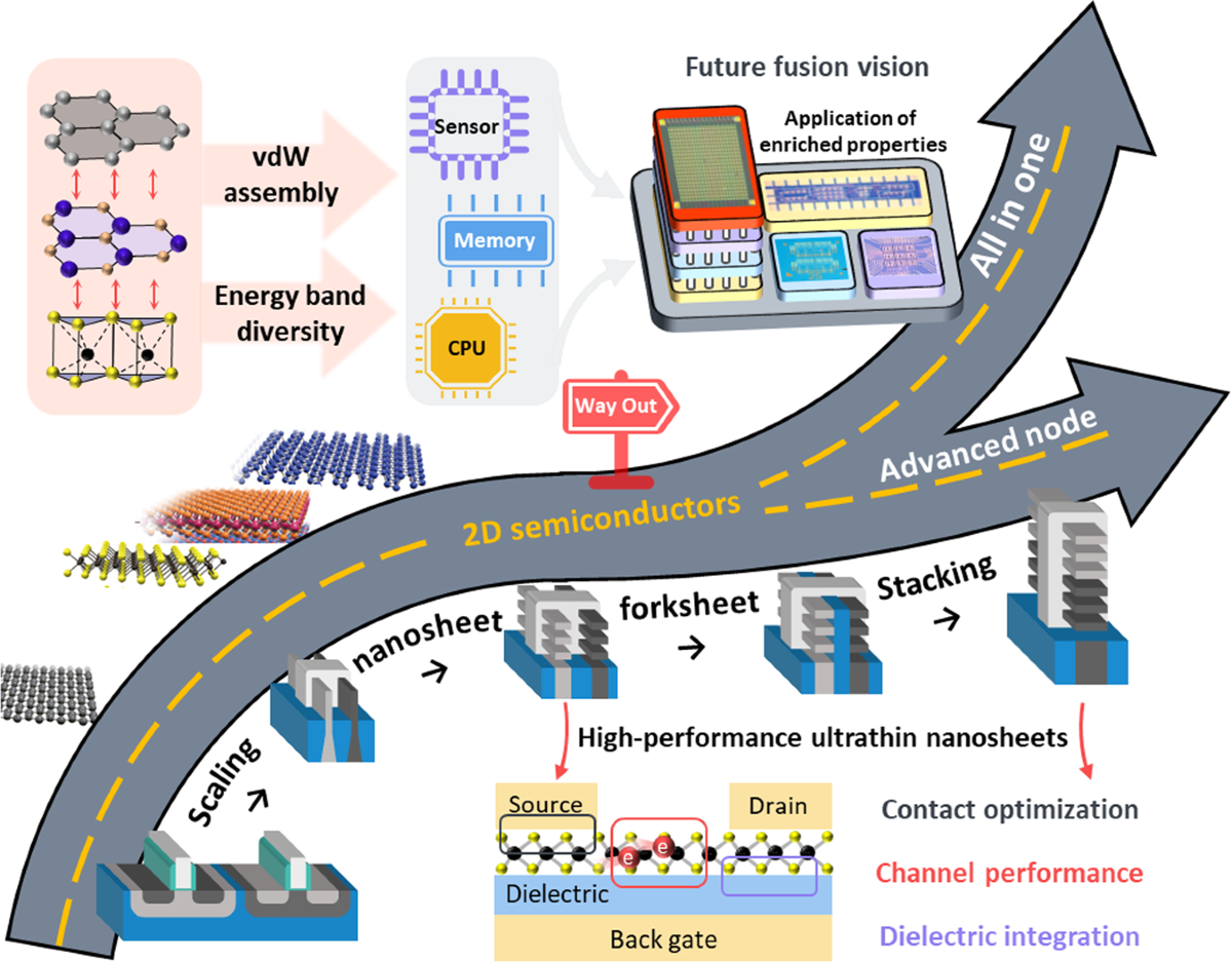
2. Structural Evolution: 2nd-Generation GAA Nanosheets + Backside Power Delivery
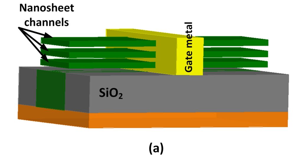
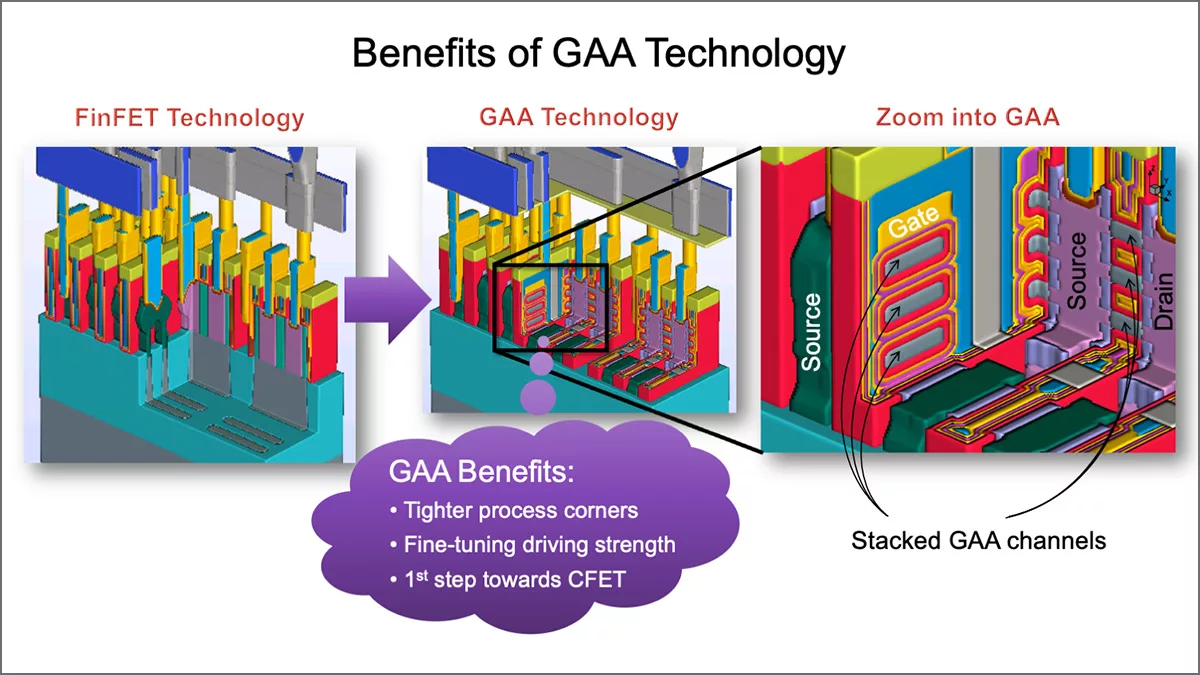
To overcome the quantum boundary, TSMC is advancing the Gate-All-Around (GAA) architecture with second-generation nanosheet designs:
- The gate fully surrounds the channel on all sides, dramatically improving electrostatic control and suppressing short-channel effects and quantum tunneling.
- Compared to FinFETs (three-sided control), GAA offers superior switching behavior and leakage reduction.
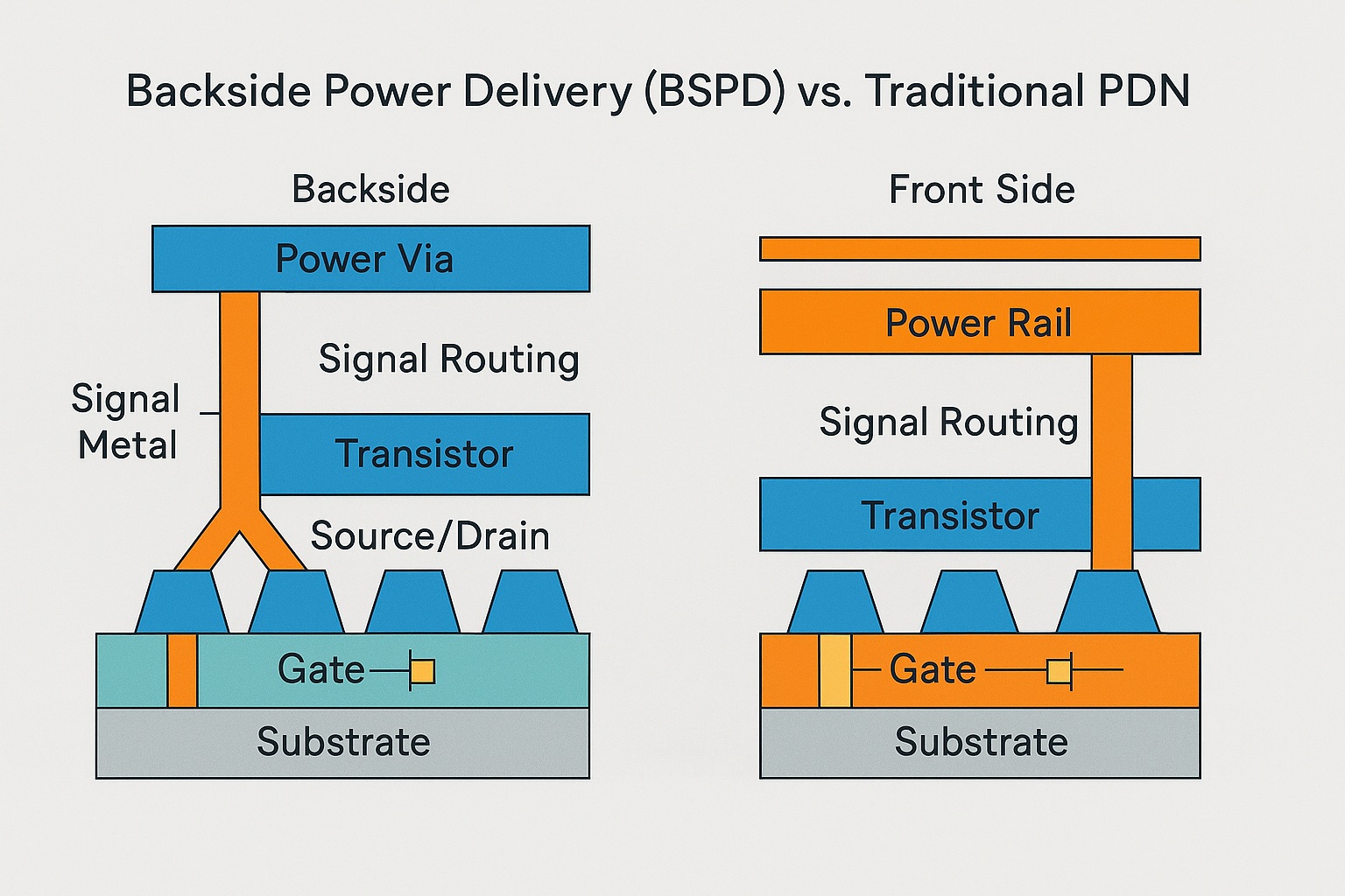
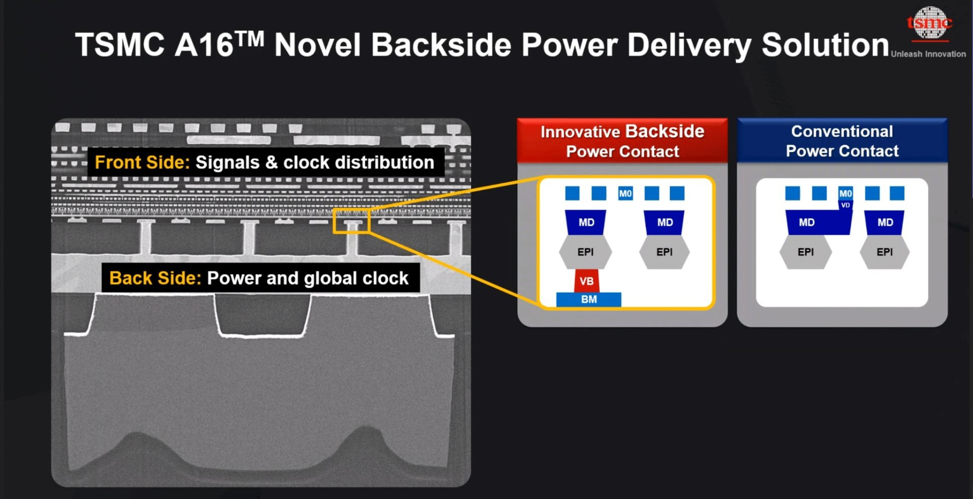
Vertical Power Delivery (Super Power Rail / Backside Power Delivery, BSPDN)
The baseline A14 node adopts a conventional frontside power delivery scheme. However, TSMC plans to introduce an advanced version—A14P—around 2029, integrating Super Power Rail technology.
This approach moves power routing to the backside of the chip, allowing the frontside to focus entirely on signal interconnects. The result is reduced electrical noise, lower IR drop, and further improvements in logic density.
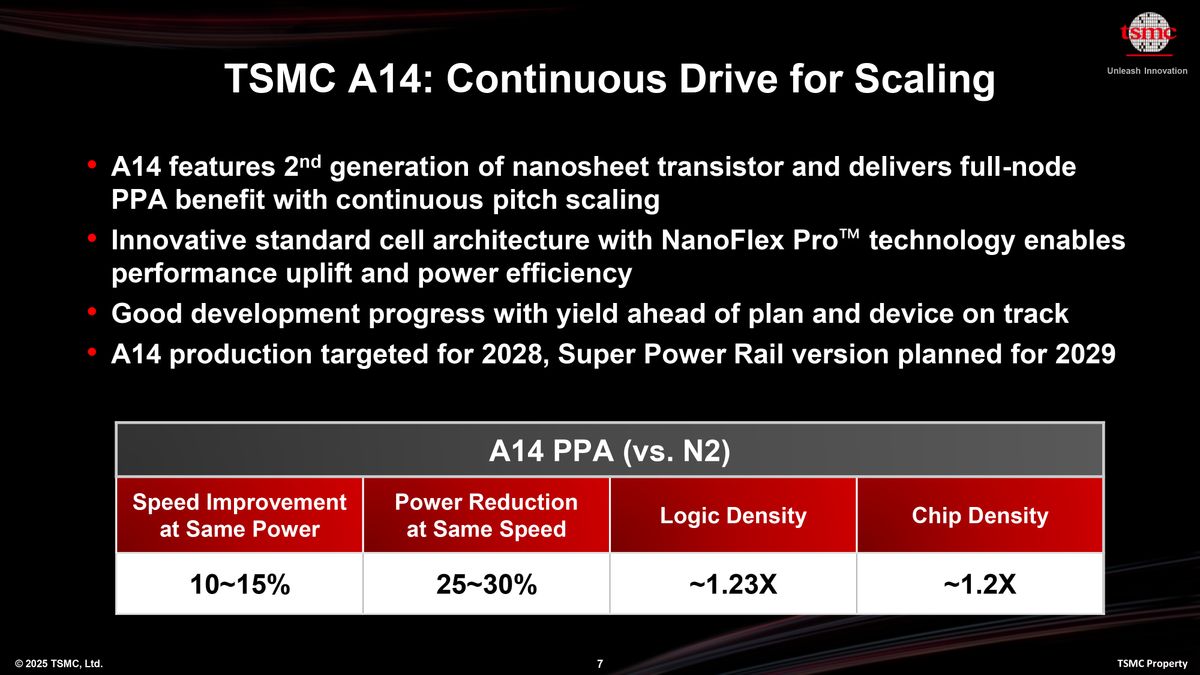
3. Key Technical Metrics and Timeline of A14
According to TSMC’s official data, A14 achieves a full-node improvement over the N2 (2 nm) process:
| Metric | Improvement vs. N2 |
|---|---|
| Performance (Speed) | +10–15% (at the same power) |
| Power Consumption | −25–30% (at the same speed) |
| Logic Density | ~1.23× increase |
| Chip Density | ~1.2× increase |
Timeline:
- Late 2027: Risk production
- 2028: Mass production (HVM)
- 2029: Introduction of Super Power Rail (backside power delivery) variant
In addition, TSMC is introducing the NanoFlex Pro standard cell architecture, enhancing design flexibility and enabling further optimization of PPA (Power, Performance, Area).
4. Beyond Silicon: Exploration of Next-Generation Materials
The atomic spacing of silicon is approximately 0.5 nm, meaning that a 1.4 nm channel can accommodate only about three atoms across its width. At this scale, physical limits are rapidly being approached.
To address this, TSMC and the broader semiconductor industry are actively exploring post-silicon materials:
-
Two-dimensional (2D) transition metal dichalcogenides (TMDs)
Materials such as molybdenum disulfide (MoS₂) and tungsten diselenide (WSe₂) offer atomic-scale thickness, providing excellent electrostatic control and significantly reduced leakage current. -
Carbon Nanotubes (CNTs)
With extremely high carrier mobility and low operating voltage, carbon nanotubes are strong candidates for future transistor channel materials.
These research directions aim to maintain high performance and low power consumption even at extremely small geometries, further mitigating the impact of quantum tunneling effects at advanced technology nodes.
留言
張貼留言